
纳米级NiAl–(Cr,Mo)共晶复合材料中的相和亚晶面分布
引言
共晶NiAl–(Cr,Mo)复合材料因其具有高熔点、良好的抗氧化性和低密度,在高温使用材料选择上非常有前景。其微观结构由有序的B2 NiAl基体和无序的体心立方(bcc)(Cr,Mo)固溶增强体组成。晶体学上,B2结构类似于bcc,其中Ni和Al分别对应两个可互换的bcc子晶格。这种相似性,加上细小的特征尺寸,使用常规电子背散射衍射(EBSD)进行相识别和获得纳米尺度取向面分布变得非常具有挑战性。
在本文中,我们使用透射式Kikuchi衍射(TKD)结合能量色散X射线谱(EDS),并比较霍夫标定(HI)、球形标定(SI)以及结合EDAX® ChI Scan™ EDS辅助相鉴定)的SI,以获得相分布并揭示经过蠕变测试的纳米级共晶NiAl–(Cr,Mo)合金的亚晶结构。
方法
材料加工:使用Bridgman工艺铸造了共晶NiAl–(Cr,Mo)合金,材料经过蠕变测试后进行了测试。
样品制备:通过镓离子束电镜(FIB)提取制备了一块电子透明的薄片。
TKD-EDS 数据采集:TKD 和 EDS 数据是通过 EDAX® Velocity™ EBSD 探测器和 EDAX Octane Elect EDS 探测器同时采集的,这些设备由 EDAX APEX 软件控制。此过程中,采集了 7 x 6 微米的区域,步进大小为 10 纳米,样品相对于水平面倾斜了 20°。
标定和后处理:花样最初通过霍夫标定进行了标定,随后通过球形标定重新标定,并通过带有ChI Scan的球形标定进行精修,ChiScan是将EDS的元素信息加入以进行相鉴定的方法,整个过程在EDAX OIM Analysis™(v 9.1)软件的OIM Matrix™模块中实现。
结果与讨论
取向面分布
霍夫标定的反极图(IPF)面分布显示了误标的像素,特别是在晶界和变形区域。球形标定减少了这些误标,取向图更干净,边界更清晰(图1)。
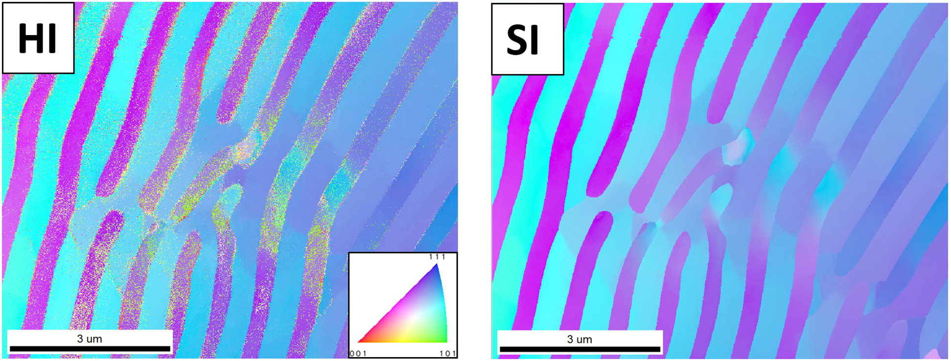
Figure 1. IPF ND orientation maps of the TKD dataset. Left) Initial Hough indexing shows scattered misindexed pixels at boundaries and in high strain regions. Right) Spherical indexing suppresses these artifacts and sharpens boundary definition.
亚晶结构
从HI得到的KAM图(图2)难以区分亚晶粒。SI标定后角度精度更高,显示了小角度的亚晶界,而这些边界在HI KAM图中被噪声掩盖。
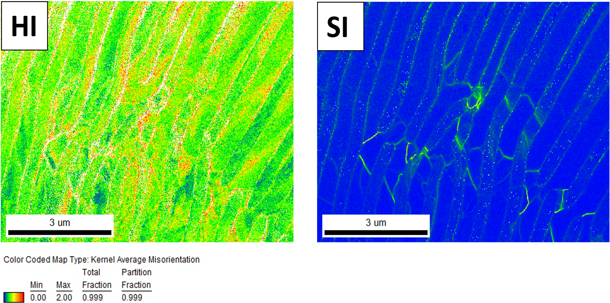
Figure 2. KAM maps (0 – 2°) created from HI (left) and SI (right). The improved orientation precision with SI resolves low angle subgrain boundaries that appear diffuse or fragmented in the HI based map.
没有EDS辅助标定的相分布图
由于B2 NiAl和bcc (Cr,Mo)在晶体结构上很相似,HI和SI都在区分这些相时遇到了困难。SI的结果相对于HI略有改善,但相鉴定错误仍然存在(图3)。B2和bcc的模拟主花样在条带强度上仅显示出细微差异,而在这些条件下收集的实验电子背散射花样(EBSPs)则没有显示出强烈的细微结构对比(图4)。这解释了为什么纯基于花样标定的方法在这个合金的相鉴定上存在困难。
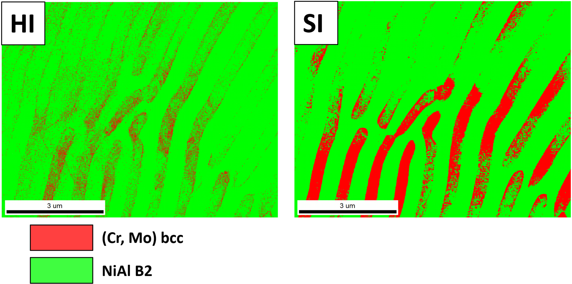
Figure 3. Phase maps produced with HI (left) and SI (right). Due to the crystallographic similarity of B2 NiAl and bcc (Cr,Mo), SI yields only a modest improvement and some misassignments persist.
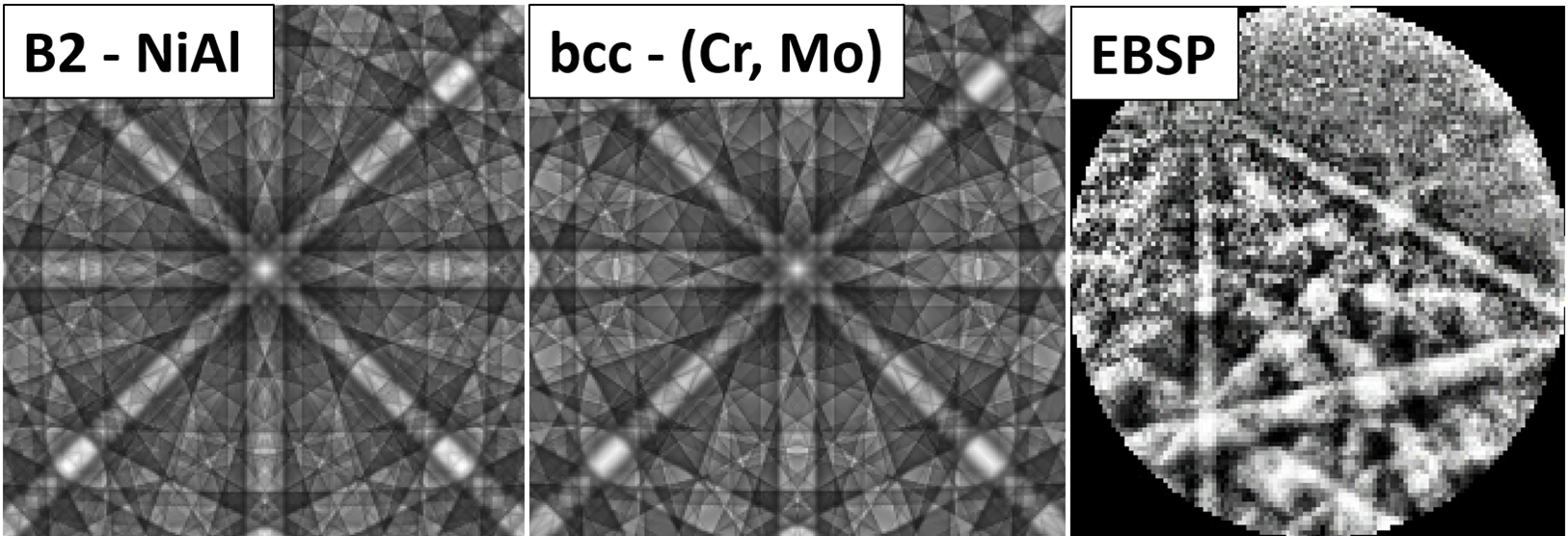
Figure 4. Simulated master patterns for B2 NiAl and bcc (Cr,Mo) exhibit only subtle band intensity differences; the representative experimental EBSP lacks the fine structure contrast needed for reliable phase discrimination.
EDS辅助标定(ChI-Scan)
一个混合元素的EDS面分布清晰地划分了NiAl富集区域和(Cr, Mo)富集区域。在SI重新标定期间通过ChI扫描整合这一元素含量因素,能够正确地进行相分配而不影响结果取向质量(图5)。
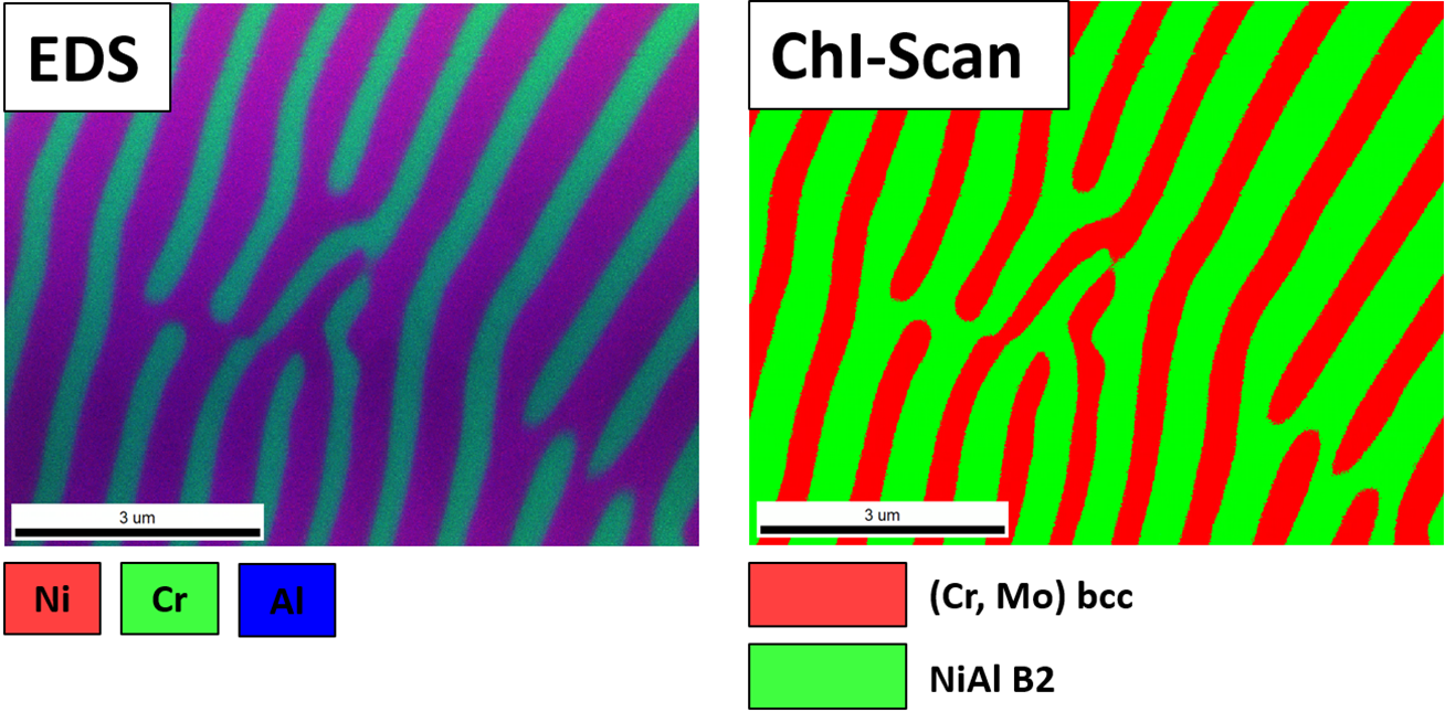
Figure 5. Blended EDS map (NiAl in purple; (Cr,Mo) in green) used during SI with ChI-Scan. Incorporating elemental context enables correct phase assignment in the final phase map while maintaining orientation quality.
结论
TKD 提供了探测共晶 NiAl–(Cr,Mo) 复合材料中纳米层所需要的空间分辨率。相较于 Hough 标定,球形标定增加了标定成功率和取向精度。ChI-Scan 利用 EDS 信号,将仅仅通过花样标定方法无法可靠区分的晶体结构相准确分开。这些硬件和软件工具结合在一起,成功提示出此纳米合金中的相、取向和小角度亚晶的分布。
致谢
我们感谢Steffen Neumeier博士(弗里德里希·亚历山大 埃尔朗根-纽伦堡大学,材料性能研究所)提供样品,以及Johan Westraadt博士(俄亥俄州立大学电子显微镜与分析中心)进行的表征和分析。