
ChI-Scan — 了解多相样品中的微观结构及量化的捷径
导言
表征样品中化合物和/或相的微观结构使分析人员能确定其加工过程和材料特性之间的关系。 在过去的 20 年中,电子背散射衍射 (EBSD) 花样分析和能量色散光谱 (EDS) 已证明是开发改进材料性能的有用工具。
然而,这些技术常常单独使用,大大降低了分析的有效性,显著增加了分析时间,或者需要更多的专业分析。 借助化学辅助扫描 (ChI-Scan™),从 EDS 获得的元素信息联合 EBSD 测量的晶体学分析,自动对所有存在的相进行准确的微观结构分析。
ChI-Scan的优势
- 区分具有相同立方晶体结构和相似晶格常数的组成相
- 当区分具有相同晶体结构和不同晶格常数的相时,将数据采集时间从数小时减少到数分钟
- 避免因样品制备和/或塑性变形导致的不确定结果
- 基于可用晶体结构的分析可将处理时间缩短十倍
- 可分析样品中存在的所有相
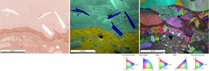
Figure 1. ChI-Scan analysis enabled the texture of a polyphase mineral to be exposed. Using ChI-Scan, two distinct rhodochrosite phases were discovered through variation in the iron content (left). The phase map (center) shows low-iron rhodochrosite (cyan), high-iron rhodochrosite (yellow), and other phases, including barium sulfate (blue), quartz (red), and pyrite (green). IPF Orientation combined with Image Quality map of the same sample (right).
ChI-Scan
EBSD 识别材料内所分析点的晶体结构和取向,揭示详细的微观结构信息。 然而,当样品中存在具有相似晶体结构的两个或多个相时,可能难以识别正确的结构。 ChI-Scan 利用来自 EDS 的成分信息将每个测量位置的候选晶体结构减少到仅具有适当化学成分的晶体结构,从而解决不确定性问题。 由于放宽了对高质量 EBSD 数据(信噪比和分辨率)的要求,因此可以区分相似晶体结构的相并加快数据采集速度。 使用 ChI-Scan,可分析有 10 多个独特相的微观结构。
微观分析结果
在此示例中, ChI-Scan 在印刷电路板金属互连的微观结构分析中非常重要。 该结构是使用铜和可伐合金多步电化学沉积来制备的。 Kovar 是一种铁镍钴合金,其热膨胀系数与硼硅酸盐玻璃相似。在电子工业中通常用于粘合到硬玻璃外壳上的金属部件。 要了解和控制加工对两种材料性能的影响,了解它们的微观结构非常重要,尤其是晶粒尺寸分布。
当单独进行分析时,使用 EDAX Velocity™ Plus EBSD 检测器进行 EBSD 分析成功地标定了 99.8% 的点,提供了高质量的取向图,揭示了详细的微观结构信息,例如晶粒尺寸、晶体取向和孪晶界。 然而,由于这两个相之间晶体结构的相似性,不可能了解每个相的微观结构及其关系。 相图揭示了两个面心立方 (FCC) 相的随机选择,对应于铜和可伐合金,但与观察到的微观结构特征无关。 铜和可伐合金都是 FCC 结构,具有相同的衍射平面和相似的晶格常数,因此很难用 EBSD 进行区分。
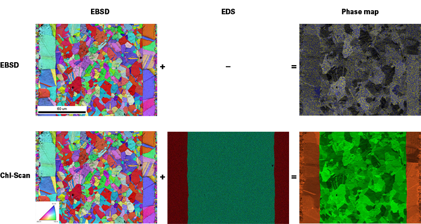
Figure 2. (EBSD column) EBSD orientation maps were collected at >3,000 indexed points per second using a Velocity Plus EBSD Detector. (EDS column) Elemental map by EDS was collected simultaneously with EBSD data using an Octane Elect Super Detector. Colorized to display copper (red), iron (green), and nickel (blue). (Phase maps column) Phase maps were determined from data. Colorized to display copper (top - blue, bottom - orange) and Kovar (top - yellow, bottom - green).
然而,同时采集元素图和使用 ChI-Scan 进行分析可以区分铜和可伐合金并生成准确的相图。 也可以进行定量微观结构分析,两个相的晶粒尺寸分布如图 2 所示。
铜相具有双峰晶粒尺寸分布,较大的晶粒靠近可伐合金界面而较小的晶粒远离它,表明在沉积过程中有两种不同的活跃的沉积和晶粒生长机制。 Kovar 相具有更均匀的晶粒分布。 对晶粒取向差的分析表明,可伐合金相具有显著的孪晶存在(相内约 50% 的晶界)。 铜相的孪晶界要少得多(约 7%)。 如果没有 ChI-Scan 提供的准确相区分,就不可能进行这种类型的详细分析。
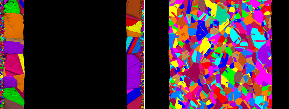
Figure 3. EBSD grain maps for the copper phase (left) and Kovar phase (right) showing a bimodal grain structure for the copper phase.
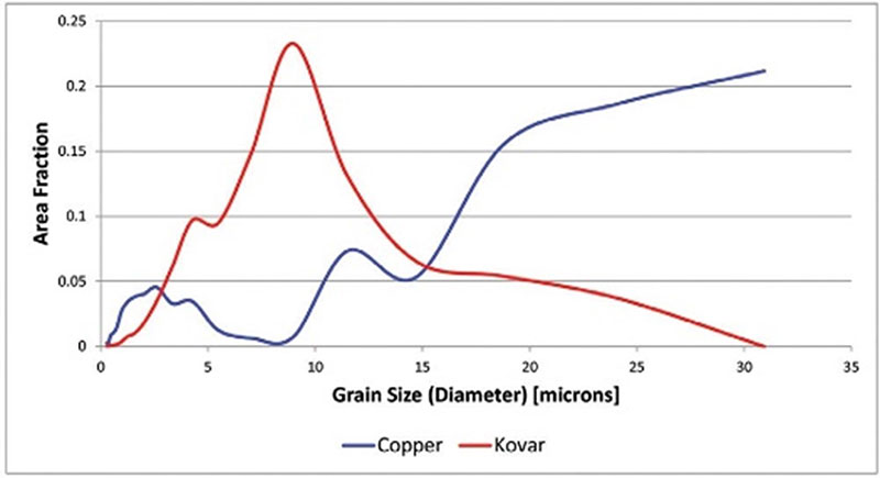
Figure 4. Grain size distributions for the copper and Kovar phases.
结论
EDAX Pegasus 系统中的 ChI-Scan 功能可实现:
- 通过消除EBSD花样分析中的不确定性结果,为科学家和工程师提供准确的相分布来表征多相材料
- 不需要高质量的EBSD花样即快速确定关键数据
- 改进了对材料中所有相的定量分析的分析
ChI-Scan 可用于金属、陶瓷、半导体和地质样品,包括(但不限于)钢中的碳化物分析、稀土磁体中的氧化物相鉴定、航空合金中的夹杂物分析以及铜矿石轴承中的矿物分析 岩石等应用。
ChI-Scan 需要使用 EDAX EDS 和 EBSD 检测器同时采集 EDS 和 EBSD 数据。